Next-Gen Display Tech: Boosting 2D Emission with Plasmonic Metasurfaces
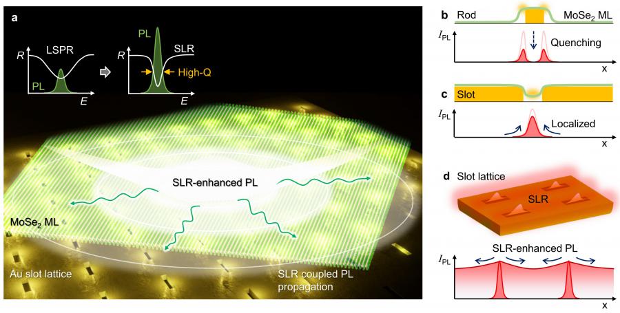
GA, UNITED STATES, June 23, 2025 /EINPresswire.com/ -- To overcome quenching and spatial localization in conventional plasmonic antenna–2D semiconductor hybrids, a plasmonic metasurface was developed. By applying Babinet’s principle to design hollow nano-antennas and inducing surface lattice resonances (SLRs), the research team minimized non-radiative losses and achieved large-area emission enhancement. This work presents a scalable approach for realizing low-power, high-brightness light emission in flexible optoelectronic devices.
van der Waals materials (vdWMs) have garnered increasing attention from both academia and industry due to their atomic-scale thickness, mechanical flexibility, and superior electrical and optoelectronic properties compared to conventional silicon-based materials. Consequently, leading semiconductor manufacturers such as TSMC and Intel are investing heavily in research and development to incorporate 2D semiconductors into next-generation devices. However, the practical implementation of vdWMs in optoelectronic applications—particularly in light-emitting devices—has been hindered by key challenges, including low quantum yield and inefficient large-area integration.
In response, a collaborative research team led by Prof. Kyoung-Duck Park (Department of Physics and Semiconductor Engineering at POSTECH) and Prof. Junsuk Rho (Departments of Mechanical Engineering, Chemical Engineering, and Electrical Engineering at POSTECH), in collaboration with Prof. Vasily Kravtsov (School of Physics and Engineering at ITMO University) has developed a plasmonic metasurface integrated with vdWMs. This novel platform addresses critical limitations of conventional plasmonic antenna–vdWM hybrids, including emission quenching and strong spatial localization. The results(doi: https://doi.org/10.1038/s41377-025-01873-3 ) of this work were recently published in Light: Science & Applications.
In pursuit of high-efficiency, low-power flexible displays, the team tackled the fundamental challenge of enhancing light emission in monolayer semiconductors. Existing strategies using metallic nanoantennas face two major drawbacks: (1) substantial non-radiative losses at the metal–semiconductor interface, and (2) the enhancement is typically localized to areas around ~100 nm², dispersed inconsistently on the 2D surface.
To overcome these challenges, the researchers designed and fabricated plasmonic metasurfaces composed of hollow slot antennas, using Babinet’s principle and Rayleigh’s anomaly. This new platform maximizes radiative decay rate and induce non-local photo-excitation in a MoSe2 monolayer. In contrast to isolated nanoantenna effects, surface lattice resonance (SLR) of slots extends optical coherence and field enhancement over larger areas, enabling large-area, high-brightness emission at low power. For emitted PL coupled with SLR, locally enhanced by up to 1600-fold, the researchers investigate its in-plane directivity and long-range propagation using angle- and space resolved spectroscopic PL measurements. The experiment reveals that a nearly 800 𝜇m2 2D luminescent sheet can be achieved regardless of the size of the MoSe2 crystal, even with a sub-𝜇m2 flake.
The researchers emphasized the broader vision, stating, “People are now seeking display technologies that go beyond IMAX—toward immersive, ultra-large-scale platforms like the Las Vegas Sphere. Next-generation displays must be flexible, low-power, high-brightness, and capable of large-area emission. This work represents a critical milestone in overcoming the limitations of 2D semiconductors and paves the way for future display and optical communication technologies.”
Also, “By integrating Babinet’s principle and surface lattice resonances into a novel metasurface architecture, we present a fundamentally new design that overcomes longstanding limitations of conventional plasmonic systems. This platform is poised to become a core technology in future high-brightness displays and photonic communication devices.”
This breakthrough is regarded as a significant step forward in redefining the future of everyday display and optoelectronic technologies.
DOI
10.1038/s41377-025-01873-3
Original Source URL
https://doi.org/10.1038/s41377-025-01873-3
Funding information
This work was supported by the National Research Foundation of Korea (NRF) grants (RS-2023-00283500, RS-2025-00559639, RS-2024-00412690), the Samsung Science and Technology Foundation (SSTP-BA2102-05), and the MSIT (Ministry of Science and ICT) under the ITRC (Information Technology Research Center) support program (IITP-2022-RS-2022-00164799). J.R. acknowledges the POSCO-POSTECH-RIST Convergence Research Center program funded by POSCO, and the National Research Foundation (NRF) grant (RS-2024-00356928) funded by the Ministry of Science and ICT (MSIT) of the Korean government. D.K.O. acknowledges the Hyundai Motor Chung Mong-Koo fellowship. J.M. acknowledges the Presidential Sejong fellow ship (RS-2023-00252778) funded by the MSIT of the Korean government. Y.Kim acknowledges the Hyundai Motor Chung Mong-Koo fellowship, and the NRF PhD fellowship (NRF-2022R1A6A3A13066251) funded by the Ministry of Education (MOE) of the Korean government. T.K. and J.K. acknowledge the support from Institute of Basic Science (IBS-R034-D1). J.K. acknowledges the support from the National Research Foundation of Korea grants (NRF-2023R1A2C2007998). This study was also supported by the MSIT (Ministry of Science and ICT), Korea, under the ITRC (Information Technology Research Center) support program (IITP-2023-RS-2022-00164799) supervised by the IITP(Institute for Information & Communications Technology Planning & Evaluation. M.T., A.N.A., and V.K. acknowledge support from Priority 2030 Federal Academic Leadership Program (angle-resolved measurements) and Russian Science Foundation, project 22-72-10047 (sample fabrication).
Lucy Wang
BioDesign Research
email us here
Distribution channels: Science, Technology
Legal Disclaimer:
EIN Presswire provides this news content "as is" without warranty of any kind. We do not accept any responsibility or liability for the accuracy, content, images, videos, licenses, completeness, legality, or reliability of the information contained in this article. If you have any complaints or copyright issues related to this article, kindly contact the author above.
Submit your press release
